
Semiconductor Testing Laboratory Architecture & Trace Metrology
Precision analytical infrastructure for semiconductor wafers, ultra-high purity process chemicals, thin-film metrology, contamination-sensitive fabrication environments, and specialized effluent treatment plants (ETP). Engineered to detect defects and impurities down to sub-nanometer and sub-ppt levels.
Wafer Geometry, Sub-Nanometer Topography & Defect Inspection
Characterizing macroscopic flatness, site-specific focal limits, and atomic lattice imperfections across 300mm silicon and wide-bandgap compound wafers.
Modern advanced node semiconductor manufacturing (sub-5nm to 2nm architectures) places unprecedented demands on starting substrate quality. As photolithographic depth-of-focus (DOF) shrinks to under 30 nm under extreme ultraviolet (EUV) exposure, microscopic wafer unflatness or surface nanotopography leads directly to focal blur, line-edge roughness, and circuit bridging.
A rigorous semiconductor testing laboratory must evaluate both geometric profile parameters (bow, warp, thickness, Total Thickness Variation [TTV], and Site Flatness Front-referenced Least-squares [SFQR]) and surface atomic finish. For compound semiconductors such as Silicon Carbide (4H-SiC), Gallium Nitride (GaN), and Gallium Arsenide (GaAs), testing must additionally identify crystalline defects including basal plane dislocations, threading dislocations, and etch pit density (EPD).
| Substrate Material | Critical Geometrical Targets | Surface Roughness (AFM) | Primary Defectivity & Metrology Tools |
|---|---|---|---|
| Prime Silicon (300 mm) | Thickness: 775 ± 20 µm Bow: < 20 µm Warp: < 30 µm SFQR: ≤ 0.025 µm |
Ra < 0.10 nm (Sub-angstrom atomic terrace finish) |
Laser surface scanning for Crystal Originated Particles (COP > 19 nm), haze mapping, and AFM verification. |
| Silicon-on-Insulator (SOI) | Top Si Layer: 12 – 70 nm (±0.5 nm) BOX Layer: 20 – 145 nm (±1.0 nm) TTV < 1.0 µm |
Ra < 0.15 nm Interface roughness < 0.2 nm |
Spectroscopic Ellipsometry for dual-layer thickness uniformity, X-ray Reflectivity (XRR) for interface density. |
| Silicon Carbide (4H-SiC, 150/200 mm) | Thickness: 350 / 500 µm Bow: < 25 µm Warp: < 40 µm |
Ra < 0.20 nm (CMP polished Si-face) | KOH molten etch for Etch Pit Density (EPD < 500 cm-2), Basal Plane Dislocation (BPD) UV photoluminescence mapping. |
| Gallium Nitride (GaN on Si/Sapphire) | Epi layer: 2 – 5 µm Radius of curvature: > 15 m Stress-induced bow control |
Ra < 0.30 nm (Atomic step bunching control) |
High-Resolution X-ray Diffraction (HR-XRD rocking curve FWHM < 250 arcsec), Cathodoluminescence defect mapping. |
Ultra-Trace Elemental Analysis & Killer Metallic Impurities
Detecting metal contaminants at sub-ppt concentrations and sub-108 atoms/cm2 on wafer surfaces to safeguard transistor gate oxide integrity.
Metallic impurities represent the primary cause of gate oxide dielectric breakdown, excessive junction leakage current, and reduced minority carrier lifetimes in semiconductor devices. Even a single trace contamination event during front-end wafer fabrication—such as the diffusion of iron (Fe), copper (Cu), or nickel (Ni) atoms into silicon crystal lattices—causes irreparable device failure.
Our semiconductor analytical laboratory designs utilize two complementary, state-of-the-art metrology methodologies:
- Vapor Phase Decomposition Inductively Coupled Plasma Mass Spectrometry (VPD-ICP-MS): Hydrofluoric acid vapor decomposes the surface native or thermal silicon dioxide film into a micro-droplet containing dissolved metallic impurities. The droplet is scanned across the wafer surface and injected directly into a Triple Quadrupole ICP-MS (ICP-QQQ) with an octopole collision cell, reaching surface detection limits of <107 to 108 atoms/cm2 for critical metals (Fe, Ni, Cu, Co, Na, K, Ca, Al).
- Total Reflection X-Ray Fluorescence (TXRF): An X-ray beam strikes the wafer surface at an angle below the critical angle of total external reflection (<0.1°), exciting only the top atomic monolayers with zero substrate background interference. This provides rapid, non-destructive wafer surface screening down to 109 atoms/cm2.
High-Purity Process Chemicals & Ultrapure Water (UPW) Verification
Evaluating SEMI C-Series Tier D electronic grade chemicals and ASTM D5127 Type E-1.1 ultrapure water standards.
Fabrication plants consume vast volumes of wet processing chemicals: hydrofluoric acid (HF) for oxide stripping, sulfuric acid (H2SO4) and hydrogen peroxide (H2O2) for piranha cleans, ammonium hydroxide (NH4OH) for SC-1 cleans, and electronic grade isopropyl alcohol (IPA) for critical drying. The purity of each delivery lot directly controls defectivity.
The semiconductor testing laboratory must verify incoming chemicals against SEMI C-Series Standards, determining trace cations, trace anions, dissolved silica, and particulate populations down to parts-per-trillion (ppt) and parts-per-quadrillion (ppq) levels.
| Purity Classification | Max Trace Impurities (per element) | Applicable Process Tier | Critical Test Methods |
|---|---|---|---|
| SEMI Grade 1 (Standard) | < 1,000 ppb (1 ppm) | Legacy packaging & non-critical wet benches | ICP-OES / Flame AA Spectrophotometry |
| SEMI Grade 2 (Advanced) | < 100 ppb | Discrete components & power semiconductors | ICP-OES / Standard ICP-MS |
| SEMI Grade 3 (VLSI Grade) | < 10 ppb | Micro-controllers & legacy memory lines | High-resolution ICP-MS & Ion Chromatography |
| SEMI Grade 4 (ULSI Grade) | < 1.0 ppb (sub-ppb) | Leading-edge 28nm – 14nm FinFET processes | Triple Quadrupole ICP-QQQ & SPOS Particle Sizing |
| SEMI Grade 5 / Tier D (Nano) | < 10 – 100 ppt (sub-ppt) | Cutting-edge sub-7nm, 3nm & 2nm GAA Foundries | VPD-ICP-MS, PFA Cleanroom Digestion, Laser LPC |
Ultrapure Water (UPW) Testing Matrix: UPW serves as the primary rinsing agent across all semiconductor cleaning, lithography, and CMP sequences. Our laboratories are equipped to measure UPW compliance according to ASTM D5127 Type E-1.1 and SEMI F63:
- Resistivity: Continuous online temperature-compensated measurement at 18.2 MΩ·cm at 25°C (approaching the theoretical purity of water).
- Total Organic Carbon (TOC): Online UV-oxidation/membrane conductometric detection with sub-1.0 ppb limit of detection.
- Dissolved Oxygen (DO): Luminescent optical sensors measuring down to <1.0 ppb DO to prevent unintended silicon oxidation.
- Reactive & Total Silica: Heteropoly blue spectrophotometry and ICP-MS measuring <0.5 ppb silica to prevent precipitation on wafer surfaces.
- Sub-30 nm Particles: High-sensitivity laser particle counters monitoring <1 particle per milliliter at >0.05 µm.
Dielectric, Metal & Nanometer Thin Film Characterization
Evaluating film thickness, refractive indices, sheet resistance, and crystal phases across atomic layer deposition (ALD) and CVD stacks.
In modern gate-all-around (GAA) nanosheets and multi-layer 3D NAND structures, functional film thicknesses often range from single atomic layers (0.3 nm) to several tens of nanometers. Characterizing physical thickness, optical bandgap, refractive index ($n$), extinction coefficient ($k$), and interfacial roughness is critical to device switching performance.
Spectroscopic Ellipsometry
Non-destructive ultra-thin film measurement:
- Wavelength Range: 190 nm to 1,700 nm (DUV to NIR).
- Thickness Resolution: Sub-angstrom (<0.05 nm) precision for gate oxides, high-k dielectrics (HfO2, ZrO2), and low-k intermetal films.
- Optical Constants: Simultaneous determination of $n$ and $k$ dispersion profiles across multi-film stacks.
Sheet Resistance & Doping
Electrical uniformity and carrier activation:
- 4-Point Probe (4PP): Automated wafer mapping of sheet resistance ($R_s$) from 1 mΩ/sq to 10 MΩ/sq.
- Eddy Current Metrology: Non-contact measurement of conductive metal films (Cu seed, barrier TiN/TaN, W plugs).
- Carrier Profiling: Capacitance-Voltage (C-V) profiling for active dopant distribution in epitaxial layers.
X-Ray Structural Analysis
Crystal phase, strain, and film density:
- X-Ray Reflectivity (XRR): Precise determination of density, thickness, and interface roughness for ultra-thin films.
- High-Resolution XRD: Epitaxial layer mismatch, relaxation, and lattice strain in SiGe and III-V heterostructures.
- X-Ray Fluorescence (XRF): Compositional analysis and thickness profiling of metallic alloy films.
Cleanroom Engineering & Airborne Molecular Contamination (AMC)
Designing ISO 14644-1 certified controlled spaces with VC-D/VC-E vibration isolation and chemical gas scrubbing.
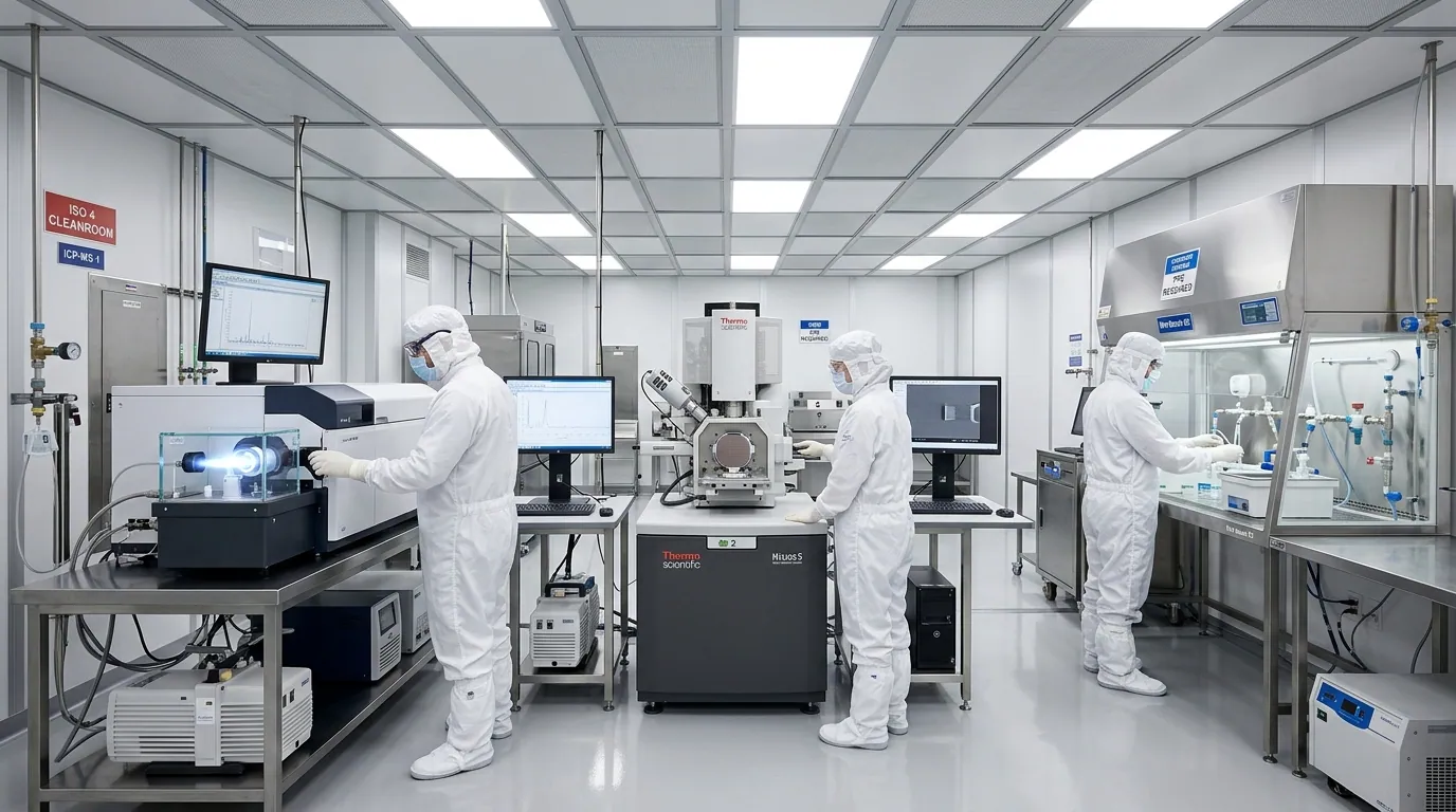
An analytical laboratory testing sub-ppb impurities cannot operate within standard industrial buildings. Ambient airborne particles, building structural vibrations, and gaseous chemical fumes will instantly distort measurement data. The laboratory environment itself is an integral part of the measurement system.
Micro-Vibration Mitigation (VC Criteria)
Vibration-free metrology bays for electron microscopy:
- Structural Foundation: Independent inertia blocks decoupled from the main building foundation.
- Vibration Criteria: Engineered to meet VC-D (6 µm/s) and VC-E (3 µm/s) vibration velocity criteria, enabling atomic-resolution SEM/TEM and AFM imaging without acoustic or mechanical smear.
- Active Pneumatic Isolation: Self-leveling pneumatic air tables dampening low-frequency building resonance.
Airborne Molecular Contamination (ISO 14644-8)
Multi-stage chemical filtration for ambient air:
- Molecular Acids (MA): Chemisorption filters capturing HF, HCl, SOx, and HNO3 to prevent wafer surface etching.
- Molecular Bases (MB): Dedicated acid-impregnated carbon stripping ammonia (NH3) and organic amines to prevent lithographic T-topping.
- Molecular Condensables (MC): Granular activated carbon capturing high boiling-point hydrocarbons and plasticizers.
- Molecular Dopants (MD): Specialized chemisorbents targeting volatile boron, phosphorus, and organometallics.
Comprehensive Analytical Instrumentation Matrix
High-precision analytical instrumentation integrated into automated, networked cleanroom data streams.
| Instrument Category | Measurement Principle | Target Parameters | Detection Threshold | Semiconductor Fab Role |
|---|---|---|---|---|
| ICP-MS (Triple Quad) | Inductively Coupled Plasma Mass Spectrometry with Octopole Cell | Trace metallic impurities (50+ elements including Fe, Cu, Ni, Na, K, Ca) | < 0.1 – 1.0 ppt (solution) < 108 atoms/cm2 (wafer) |
Process chemical QC, wafer surface cleaning verification |
| TXRF Spectrometer | Total Reflection X-Ray Fluorescence Spectrometry | Non-destructive wafer surface metallic contamination (S to U) | < 109 – 1010 atoms/cm2 | Post-clean and post-ash wafer surface screening |
| FE-SEM / EDS | Field Emission Scanning Electron Microscopy with Energy Dispersive X-Ray | Nanoscale defect imaging, cross-sectional CD, elemental identification | 0.6 nm imaging resolution; sub-micron elemental mapping | Yield failure analysis, particulate defect identification |
| Spectroscopic Ellipsometer | Multi-wavelength polarization reflection analysis (190–1700 nm) | Single and multi-layer film thickness, refractive index ($n, k$) | < 0.05 nm thickness; ±0.001 index precision |
Gate oxide, ARC, and dielectric thin film metrology |
| Atomic Force Microscope (AFM) | Tapping / contact mode atomic cantilever deflection scanning | 3D surface topography, atomic step roughness, trench profiles | Vertical resolution < 0.01 nm (sub-angstrom) | Wafer nanotopography, post-CMP micro-scratching inspection |
| Ion Chromatograph (IC) | Anion/cation separation with suppressed conductivity detection | Trace inorganic anions (F-, Cl-, NO3-, SO42-) and cations | < 10 – 50 ppt in UPW and process chemicals | UPW validation, chemical bath acid-anion monitoring |
SEMI, ASTM & ISO/IEC Quality Frameworks
Methodologies aligned with global standards to guarantee worldwide fab audit acceptance.
SEMI Global Standards
The microelectronics industry benchmark:
- SEMI C-Series: Guidelines for ultra-pure process chemicals, acids, bases, and solvents (SEMI C1, C12, C15).
- SEMI M-Series: Specifications for polished monocrystalline silicon wafers, SOI wafers, and compound semiconductors.
- SEMI F-Series: Ultrapure water (SEMI F63) and specialty gas distribution cleanliness guidelines.
ASTM International
Rigorous test protocols for electronics materials:
- ASTM D5127: Standard Guide for Ultra-Pure Water Used in the Electronics and Semiconductor Industry.
- ASTM F1397 / F1398: Test methods for moisture, oxygen, and gaseous contamination in electronic grade gas delivery systems.
- ASTM F576: Measurement of insulator thickness and refractive index.
ISO / IEC & LIMS Compliance
Accreditation and data governance:
- ISO/IEC 17025:2017: General requirements for the competence of testing and calibration laboratories.
- ISO 14644-1 / 8: Cleanroom particle classification and airborne molecular contamination (AMC).
- 21 CFR Part 11: Cryptographic audit trails, electronic signatures, and tamper-proof Certificate of Analysis (CoA) generation.
Specialized Effluent Treatment Plants (ETP) for Semiconductor Laboratory Discharges
Multi-stream segregated drainage, hydrofluoric acid (HF) precipitation, heavy metal extraction, and Zero Liquid Discharge (ZLD) reclamation.
Testing and sample preparation in semiconductor laboratories generate dangerous and strictly regulated chemical discharges. Unlike standard commercial labs, semiconductor laboratory effluent contains high concentrations of hydrofluoric acid (HF) from wafer etching, toxic heavy metals (copper, nickel, cobalt, chromium) from metallization baths, hazardous metalloids (gallium and arsenic) from compound semiconductor substrates, strong oxidizers, organic solvents, and concentrated acid/alkali washings.
Mixing these incompatible waste streams creates catastrophic safety hazards (such as toxic gas release or exothermic reactions) and makes regulatory discharge compliance impossible. BEYOND engineers dedicated, skid-mounted and centralized Semiconductor Laboratory Effluent Treatment Plants (ETP) utilizing completely segregated collection piping and tailored multi-stage physicochemical treatment trains.
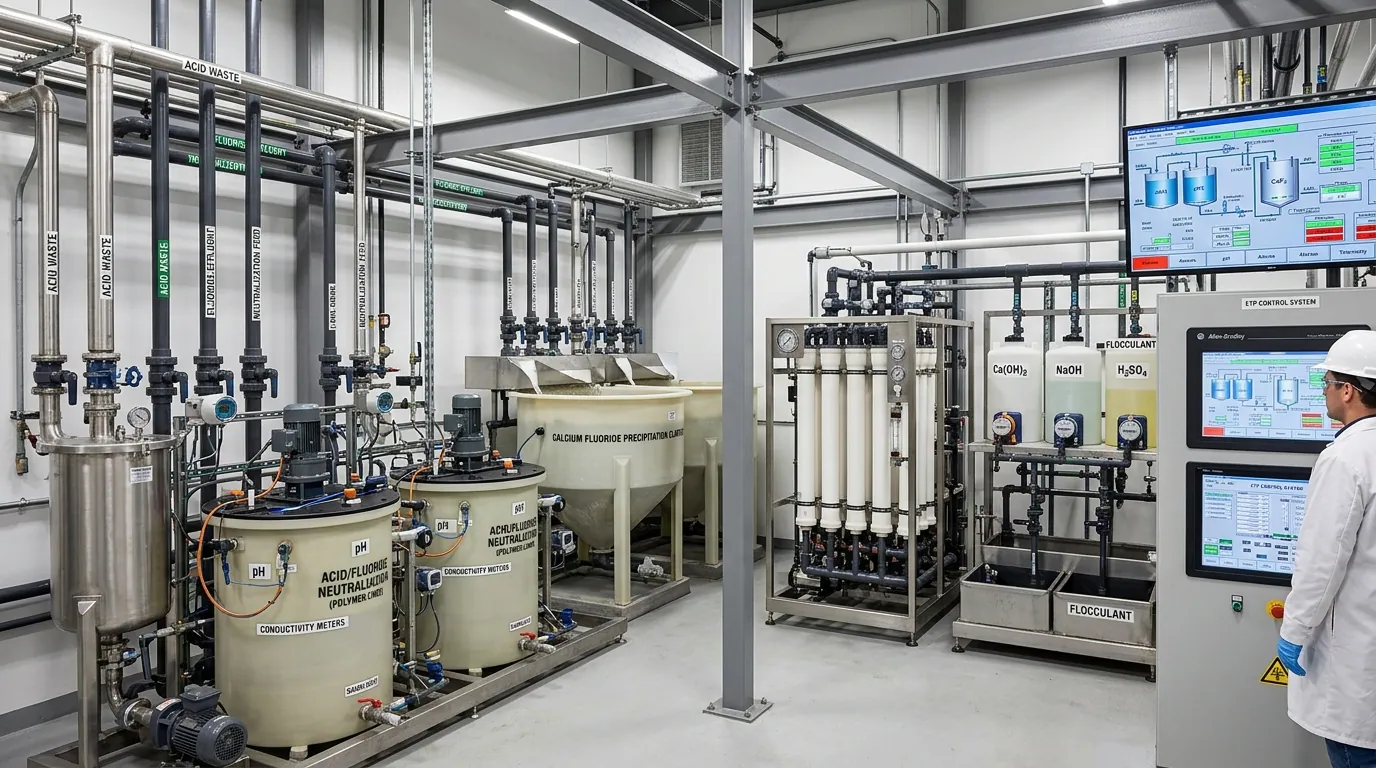
1. Hydrofluoric Acid (HF) & Fluoride ETP
Segregated fluoride precipitation to sub-5 ppm limits:
- Two-Stage Calcium Precipitation: Precision dosing of hydrated lime [Ca(OH)2] or calcium chloride (CaCl2) reacting with free fluoride ions:
Ca2+ + 2F- → CaF2↓ (Insoluble)
- Coagulant & Polymer Aids: PAC and anionic polyacrylamide bridging to flocculate micro-crystalline CaF2 precipitates.
- Lamella Clarification & Dewatering: Inclined plate clarifiers and filter presses producing dry, non-leachable calcium fluoride cake (>60% solids).
2. Heavy Metals & Toxic Metalloids (Ga/As)
Eliminating copper, nickel, gallium, and arsenic ions:
- pH-Dependent Hydroxide/Sulfide Precipitation: Precise chemical dosing insolubilizing Cu2+, Ni2+, and Co2+ as metal hydroxides.
- Gallium & Arsenic Chelation: Specialized ferric coprecipitation and selective chelating ion-exchange resin columns removing As and Ga to <0.05 mg/L.
- Microfiltration Polish: 0.1 µm tubular membranes eliminating residual colloidal heavy metal pin-flocs.
3. Automated Neutralization & ZLD Reuse
Continuous balancing, water recovery, and telemetry:
- Dual-Stage Equalization & pH Control: High-precision dosing of H2SO4 and NaOH controlled by dual-junction pH sensors, maintaining effluent at pH 6.8–7.4.
- Zero Liquid Discharge (ZLD) Recycling: Secondary RO membranes and evaporation skids recovering 85–95% of treated water for scrubber and cooling tower makeup.
- CPCB / SPCB Online Telemetry: IoT-connected real-time telemetry transmitters streaming pH, fluoride, COD, TSS, and flow directly to regulatory servers.
| Wastewater Stream | Raw Laboratory Discharge | After BEYOND Specialized ETP | Regulatory Standard (CPCB / EPA) |
|---|---|---|---|
| Fluoride Ions (F-) | 1,000 – 10,000 mg/L (toxic HF waste) | < 3.0 – 5.0 mg/L | < 5.0 – 10.0 mg/L |
| Total Heavy Metals (Cu, Ni, Co) | 50 – 500 mg/L (plating & etchants) | < 0.10 mg/L | < 1.0 – 3.0 mg/L |
| Arsenic (As) & Gallium (Ga) | 10 – 100 mg/L (III-V wafer waste) | < 0.05 mg/L (trace level) | < 0.2 mg/L |
| pH Value | Extreme (pH 0.5 to 13.5) | 6.8 – 7.4 (neutralized) | 6.5 – 8.5 |
| Total Suspended Solids (TSS) | 500 – 3,000 mg/L | < 10 mg/L (crystal clear) | < 50 – 100 mg/L |
BEYOND's Competence in Laboratory Setup: End-to-End Support in Every Possible Way
We possess the complete engineering capabilities to support your organization from greenfield conception to full operational accreditation.
Setting up a state-of-the-art semiconductor testing laboratory is one of the most demanding engineering undertakings in advanced manufacturing. It requires the seamless convergence of contamination-controlled architecture, ultra-sensitive metrology instrumentation, micro-vibration mitigation, hazardous gas and chemical distribution, and rigorous environmental waste treatment.
BEYOND has the established competence to support your project in every possible way. As a unified engineering entity with deep domain mastery across both high-purity laboratory systems and industrial environmental engineering, we eliminate the risks, delays, and finger-pointing inherent in multi-contractor models.
1. Turnkey Cleanroom & MEP Engineering
Controlling every atmospheric and structural variable:
- ISO 14644-1 Cleanrooms: Turnkey delivery of Class 1 (ISO 3), Class 10 (ISO 4), Class 100 (ISO 5), and Class 1,000 (ISO 6) testing spaces with positive-pressure cascading.
- Specialized HVAC & AMC Scrubbing: Recirculating air handling units (AHU) with terminal ULPA/HEPA filters, chemical gas adsorption (MA, MB, MC, MD), and precise climate control (±0.2°C, ±2% RH).
- Micro-Vibration Decoupled Foundations: Custom VC-D / VC-E inertia blocks engineered specifically for high-magnification electron microscopes, AFM cantilevers, and optical profilometers.
- High-Purity Utilities: PVDF loops delivering ASTM Type E-1.1 UPW (18.2 MΩ·cm), coaxial double-containment specialty gas distribution (N2, Ar, CDA, H2), and negative-exhaust chemical fume hoods.
2. Metrology Sourcing, ETP & Lifecycle Support
Complete instrumentation, compliance, and accreditation:
- Single-Vendor Metrology Sourcing: Procurement, factory testing, and site integration of ICP-MS, TXRF, FE-SEM/EDS, AFM, Ellipsometers, and IC systems.
- Validation Protocols (IQ/OQ/PQ): Comprehensive Installation, Operational, and Performance Qualification executed against certified NIST/NABL traceable reference materials.
- Integrated Specialized ETP: Full in-house design, manufacturing, and automation of the laboratory Effluent Treatment Plant (ETP)—handling HF, heavy metals, and ZLD without requiring third-party environmental vendors.
- ISO/IEC 17025 Accreditation & LIMS: Turnkey SOP authoring, measurement uncertainty budgets, quality manuals, and deployment of 21 CFR Part 11 compliant semiconductor LIMS software.
- 24/7 Long-Term Support: Preventive maintenance, ongoing calibration cycles, reagent supply, operator training, and comprehensive Annual Maintenance Contracts (AMC).
Technical Consultation & Facility Engineering
Connect directly with our semiconductor metrology engineers and cleanroom systems team. We are ready to support your laboratory setup, instrumentation sourcing, or specialized ETP wastewater requirement in every possible way.