
CMP Slurry Particle Size & Dispersion Analysis
The CMP (Chemical Mechanical Planarization) process is a crucial component of modern multilayer semiconductor manufacturing. Its ability to achieve nanoscale smoothness makes it indispensable, as both die sizes and lithographic techniques continue to shrink. Given the high costs associated with cutting-edge semiconductor device production and the pivotal role of CMP, it is no surprise that abrasive slurries used in the process undergo rigorous characterization.
The Role of CMP Slurry in Multilayer Semiconductor Manufacturing
Understanding the delicate balance between chemical etching, mechanical abrasion, and sub-nanometer surface topography.
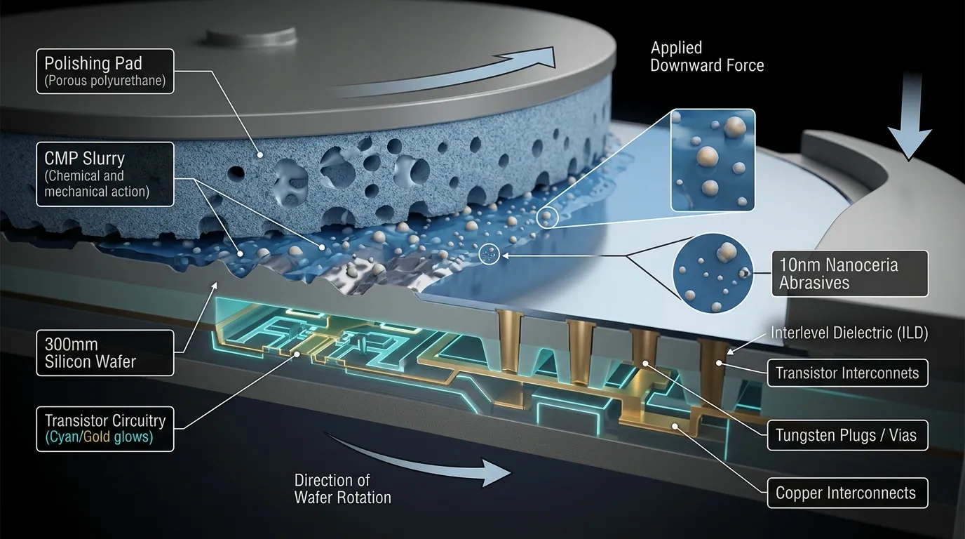
In modern high-density integrated circuit (IC) fabrication, planarization across multiple metal and dielectric layers is essential to maintain depth-of-focus during deep ultraviolet (DUV) and extreme ultraviolet (EUV) photolithography. Chemical Mechanical Planarization combines chemical reaction dynamics with mechanical abrasive force to achieve atomic-level surface flatness.
During the CMP process, slurry containing suspended nanoscale abrasive particles (such as silica, ceria, or alumina) is continuously delivered onto a rotating polyurethane polishing pad. The downward force applied to the wafer presses its microscopic circuit features against the abrasive particles, chemically softening and mechanically shearing surface peaks to achieve planarization.
Distinguishing Good Slurry from Bad to Prevent Wafer Loss
Why rigorous particle size and stability measurements safeguard millions of dollars per production lot.
A sub-standard slurry batch can contain particles that are too fine or too coarse, affecting the removal rate, or can contain a few oversized aggregates that cause micro scratches on the wafer surface. CMP slurry manufacturers and users are highly interested in particle size information. This measurement can prevent the loss of millions of dollars worth of wafers by distinguishing good slurry from bad.
Good slurry removes material at a consistent rate and uniformly across the wafer, exhibiting predictable performance because of a uniform particle size distribution with excellent stability. Conversely, a low stability slurry can quickly form large particle aggregates, causing irreparable damage to the wafer.
| Slurry Attribute | Qualified Slurry Batch (Good Slurry) | Sub-Standard Slurry Batch (Bad Slurry) |
|---|---|---|
| Particle Size Distribution | Tight, monodisperse or controlled bimodal distribution with zero coarse tail (>0.5 µm). | Broad or skewed distribution containing oversized agglomerates or excessive ultrafines. |
| Material Removal Rate (MRR) | Consistent and predictable removal rate (within ±1.5% lot-to-lot variance). | Erratic removal rates: fine particles under-polish; coarse particles over-polish unpredictably. |
| Wafer Surface Defectivity | Atomically smooth finish, zero micro-scratching, uniform dielectric layer planarity. | Micro-scratches, pits, dishing, erosion, and killer defects causing wafer scrap. |
| Colloidal Dispersion Stability | High electrostatic repulsion (zeta potential > |30| mV); stable under high-shear pumping. | Low colloidal stability; rapid flocculation, settling, and clogging of fab slurry delivery loops. |
| Economic & Fab Impact | Maximizes wafer yield, protects production lots valued at $200k–$2M+ per 25-wafer FOUP. | Catastrophic yield fallout, tool downtime, and potential millions of dollars in wafer losses. |
Standard Ceria (~100 nm) vs. Nanoceria (≤ 10 nm)
Understanding production differences and divergent analytical requirements for future CMP processes.
In the future, two major types of CMP slurries using ceria will cohabitate: standard ceria with a particle size of around 100 nm, and nanoceria with a particle size of 10 nm or less. These types of CMP slurries undergo production using different methods. Standard ceria is created by breaking down large particles into smaller ones, while generating particles directly from a liquid produces nanoceria. This production difference influences our analytical requirements.
Standard ceria, resulting from the breakdown of larger particles, has a higher concentration. We need to measure these higher concentrations, control particle size during the process, detect the endpoint, and identify any remaining large particles. For nanoceria, lower concentration measurements are necessary, along with information on the number of particles. Process control of CMP slurry is also necessary to ensure product quality.
| Parameter | Standard Ceria (~100 nm) | Nanoceria (≤ 10 nm) |
|---|---|---|
| Production Methodology | Top-down mechanical breakdown: Wet bead milling and attrition of larger cerium oxide crystals. | Bottom-up liquid synthesis: Controlled chemical precipitation and nucleation directly from liquid precursors. |
| Typical Slurry Concentration | High concentration (often 5 wt% to 30 wt% solid stock solution). | Lower working concentration (often < 1 wt% solids, high surface-to-volume ratio). |
| Primary Metrology Needs |
|
|
| Process Quality Control | High-shear recirculation stability, filter pass-through validation, and sediment re-dispersibility. | Liquid precursor chemical purity, surface functionalization tracking, and shelf-life stability. |
Slurry Particle Size Analysis of Tens of nm Using Centrifugal Sedimentation
Realizing precise particle size distribution measurement from undiluted solutions to dilute samples (10 nm to 40 μm).
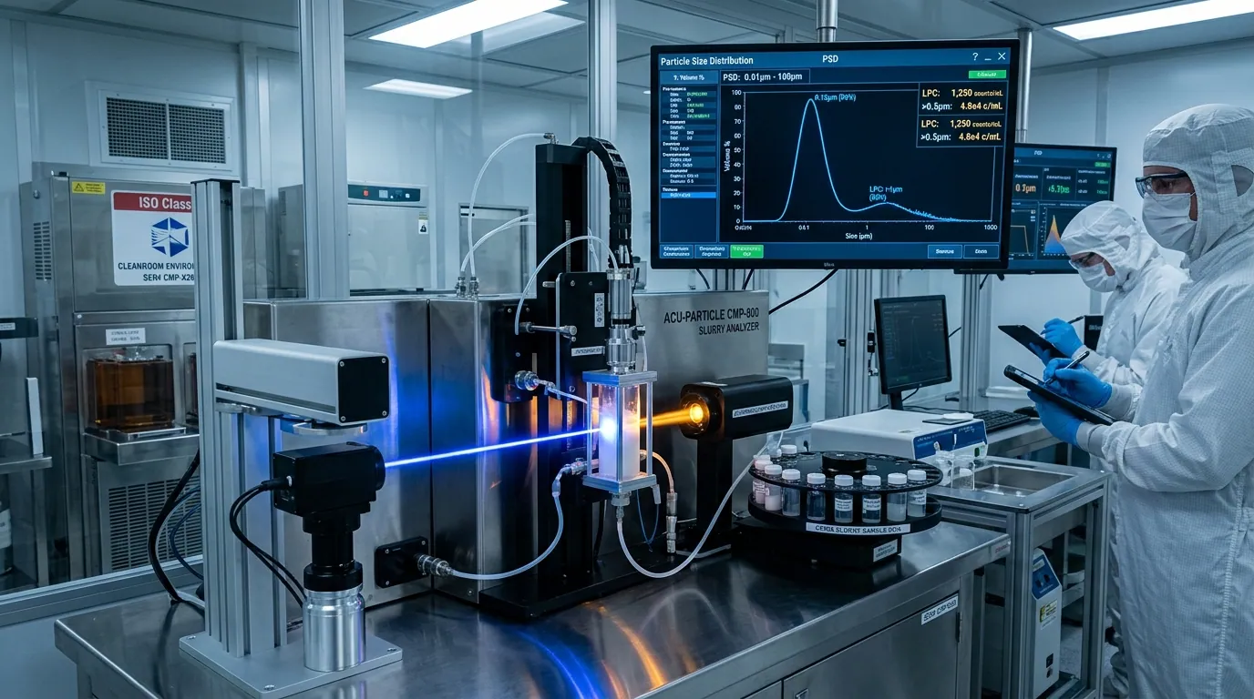
For measuring nanoparticles in the tens-of-nanometers regime, conventional laser diffraction often lacks the resolution required to distinguish subtle multi-modal peaks. The centrifugal sedimentation method utilizes high-speed centrifugal acceleration ($r\omega^2$) to separate particles according to Stokes' Law, where sedimentation velocity depends on the square of the particle diameter and the buoyant density difference.
This technique provides unmatched hydrodynamic fractionation, enabling detection of single-nanometer differences in colloidal silica and ceria. It is particularly effective for identifying the presence or absence of a coating agent on the surface of colloidal particles, capturing small amounts of foreign matter, and pinpointing killer agglomerates.
CMP Slurry Dispersibility Analysis in Stock Solution
In-situ particle dispersion analysis in undiluted slurry stock solutions without dilution shock.
In standard laboratory testing, analysts often dilute concentrated slurries with deionized water or buffer solutions to satisfy optical detector limits. However, dilution can induce severe measurement artifacts. Adding diluent alters the chemical equilibrium, shifts the pH, and reduces ionic strength—which frequently causes artificial agglomeration or conversely dissociates loose aggregates that actually exist in the production bath.
Analyzing CMP slurry in its undiluted stock solution state provides authentic insight into particle dispersibility as supplied by chemical manufacturers. In-situ optical transmission, backscattering, and centrifugal sedimentation stability profiling monitor phase separation, sedimentation velocity, and the re-dispersibility of sedimented cakes across fab delivery loops.
Dilution Artifact Risks
Why preparing diluted samples often produces misleading analytical data:
- pH Shock: Diluting changes the local pH, altering the particle surface charge and causing false agglomeration.
- Ionic Strength Collapse: Decreasing salt concentration compresses or expands the electrical double layer abnormally.
- Surfactant Desorption: Dispersants and stabilizing polymers desorb from the particle surface upon dilution.
Undiluted Stock Solution Benefits
Key advantages of direct stock solution dispersibility characterization:
- True In-Situ State: Evaluates the genuine dispersion state experienced in fab chemical supply systems (SDS).
- Shelf-Life Prediction: Accurately measures sedimentation rate and cake formation kinetics over storage time.
- Shear Degradation: Measures particle stability under high-shear recirculation pumping before wafer application.
Particle Zeta Potential Analysis & Impurity Inspection in GaAs Wafers by Cathodoluminescence
Connecting colloidal surface charge metrology to microscopic wafer crystal integrity.
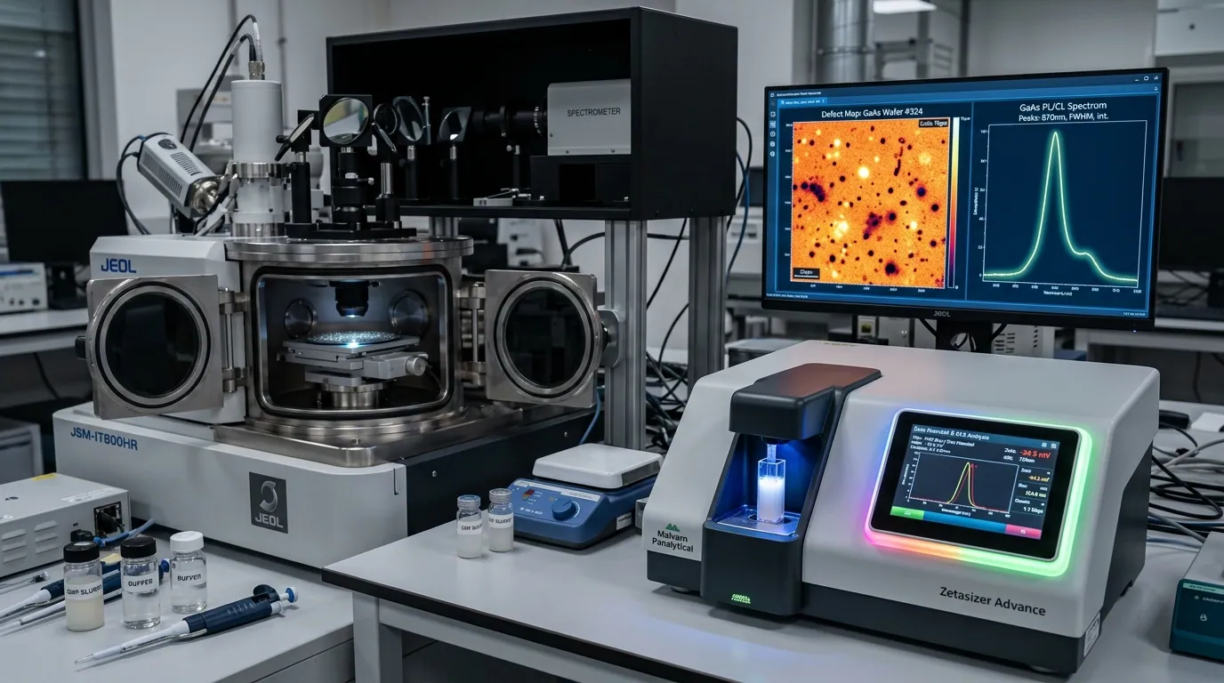
Zeta Potential in CMP Slurries: Zeta potential quantifies the electrostatic potential at the slipping plane of colloidal particles. A zeta potential magnitude exceeding ±30 mV creates strong electrostatic repulsion between adjacent particles, preventing agglomeration. Furthermore, the zeta potential governs the electrostatic affinity between abrasive particles and specific wafer surface films (such as SiO2, Si3N4, Cu, or tungsten), directly dictating the chemical removal rate.
Compound Semiconductor Wafers & Cathodoluminescence: When polishing advanced compound semiconductors such as Gallium Arsenide (GaAs), wafer surface requirements are extraordinarily strict. A sub-standard slurry batch not only causes surface scratches, but also introduces subsurface lattice strain, point defects, and chemical impurities that destroy high-frequency device performance.
Cathodoluminescence (CL) Spectroscopy: By combining an electron beam excitation source with a high-resolution optical spectrometer, cathodoluminescence images non-radiative recombination centers and point defect distributions in polished GaAs wafers. Defective slurry particles that introduce crystal dislocations or metallic impurities appear immediately as dark spots or wavelength-shifted peaks on the cathodoluminescence spectral map.
Analytical Instrumentation & Measurement Physics Matrix
Comprehensive instrument cluster for turnkey semiconductor CMP laboratory integration.
| Instrument / Technique | Measurement Physics | Measuring Range | Sample Condition | Key Semiconductor Benefit |
|---|---|---|---|---|
| Centrifugal Nanoparticle Sizer | Centrifugal sedimentation & Stokesian separation | 10 nm to 40 μm | Undiluted to dilute | Separates single-nm differences; detects killer LPC tail. |
| Zeta Potential Analyzer | Phase Analysis Light Scattering (PALS) | -200 mV to +200 mV | Dilute to concentrated | Evaluates colloidal stability (>|30| mV) and pH isoelectric points. |
| Dynamic Light Scattering (DLS) | Brownian motion & photon correlation spectroscopy | 0.3 nm to 10 μm | Dilute solutions | Rapid screening of hydrodynamic diameter (Dh) and polydispersity (PdI). |
| Laser Diffraction Analyzer | Fraunhofer & Mie light scattering | 10 nm to 3,000 μm | Wet circulation | Broad dynamic range particle size distribution and span metrics. |
| Cathodoluminescence (CL) System | Electron-beam stimulated photon emission | Sub-micron spatial, UV-VIS-NIR | Polished wafer substrate | Maps subsurface crystal lattice damage & impurities in GaAs wafers. |
| ICP-MS Spectrometer | Inductively coupled plasma mass spectrometry | Sub-ppt detection limit | Digested liquid slurry | Quantifies trace metal contamination (Fe, Cu, Ni, Na, K, Ca). |
| Cone-Plate Micro-Rheometer | Rotational shear stress & strain rate | 0.1 to 100,000 s⁻¹ shear | Undiluted slurry | Profiles shear-thinning and high-shear viscosity on polishing pads. |
Standardized CMP Slurry Quality Assurance Pipeline
Rigorous 9-step testing protocol from incoming raw material receipt to validated Certificate of Analysis (COA).
Phase 1: Receipt & Dispersion
Ensuring sample integrity and authentic colloidal character:
- Step 01: Chain-of-custody barcode logging and lot verification.
- Step 02: Temperature stabilization and controlled low-shear mixing.
- Step 03: Undiluted stock solution dispersibility and sedimentation check.
Phase 2: Particle & Surface Metrology
Precise hydrodynamic and electrostatic characterization:
- Step 04: Centrifugal sedimentation sizing (tens of nm resolution).
- Step 05: Zeta potential determination across operating pH levels.
- Step 06: Large Particle Content (LPC > 0.5 µm tail) quantification.
Phase 3: Chemistry & Wafer Validation
Purity testing and post-polish wafer inspection:
- Step 07: Chemical assay (pH, conductivity, solids wt%, oxidizer decay).
- Step 08: Ultra-trace metal impurities via ICP-MS (ppt detection).
- Step 09: Post-CMP wafer inspection (Cathodoluminescence on GaAs).
Specialized Effluent Treatment Plants (ETP) for CMP Slurry Laboratory Discharges
Engineered multi-stage treatment architectures for colloidal nanoparticle destabilization, chemical oxidizer quenching, and Zero Liquid Discharge (ZLD) reclamation.
Laboratory characterization and testing of CMP slurries generate highly specialized effluent streams that conventional industrial wastewater treatment plants cannot process. Because CMP slurries are engineered to maintain extreme colloidal stability (with high zeta potential preventing settling), waste rinsewaters and rejected sample matrices carry stable suspended nanoparticles (nano-ceria ≤10 nm, colloidal silica, and fumed alumina) alongside potent chemical additives: hydrogen peroxide (H2O2), organic complexing acids, pH buffers (KOH, NH4OH, organic amines), and copper corrosion inhibitors such as benzotriazole (BTA).
Direct discharge of untreated CMP laboratory effluent causes severe fouling of municipal drainage, regulatory violations, and environmental contamination. BEYOND engineers dedicated, skid-mounted and centralized CMP Slurry Effluent Treatment Plants (ETP) that eliminate colloidal turbidity, destroy chemical oxidants, dewater abrasive solids, and recycle treated water back into facility utilities.
1. Colloidal Destabilization & Coagulation
Overcoming electrostatic repulsion to aggregate nano-abrasives:
- Charge Neutralization: Precision dosing of polyaluminum chloride (PAC) and ferric chloride to collapse the electrical double layer.
- Polymeric Flocculation: High-molecular-weight cationic/anionic polymer bridging creating dense, heavy micro-flocs.
- Electro-Coagulation Skids: Sacrificial iron/aluminum electrodes for rapid destabilization without excessive chemical sludge.
2. Chemical Oxidation Quenching & TOC Removal
Neutralizing active chemistry and complexing reagents:
- Catalytic H2O2 Decomposition: Manganese dioxide (MnO2) fixed-bed catalytic reactors and sodium bisulfite dosing to safely extinguish peroxide.
- BTA & Organics Adsorption: Granular Activated Carbon (GAC) polishing beds stripping benzotriazole and organic carboxylic acids.
- Automated Dual-Stage pH Neutralization: PID-controlled acid (H2SO4) and caustic (NaOH) dosing maintaining pH 6.5–8.5.
3. Membrane Ultrafiltration & ZLD Recycling
Sub-nanometer particle separation and dry cake recovery:
- Ceramic Ultrafiltration (UF): High-shear crossflow silicon carbide/alumina membranes achieving >99.9% turbidity removal.
- Filter Press Dewatering: Heavy-duty recessed plate filter presses producing dry, non-leachable abrasive filter cakes (>50% solids).
- Zero Liquid Discharge (ZLD): Secondary Reverse Osmosis (RO) recovering high-purity permeate for wet scrubbers and cooling towers.
| Effluent Parameter | Raw CMP Lab Discharge | After BEYOND Specialized ETP | CPCB / EPA Regulatory Limit |
|---|---|---|---|
| Total Suspended Solids (TSS) | 1,500 – 15,000 mg/L (colloidal) | < 10 mg/L (clear permeate) | < 50 – 100 mg/L |
| Turbidity | > 2,500 NTU (milky white) | < 1.0 NTU (crystal clear) | < 10 NTU |
| Residual Peroxide (H2O2) | 500 – 5,000 mg/L | < 1.0 mg/L (quenched) | < 5.0 mg/L |
| pH Level | Extreme (pH 2.0 to 11.5) | 6.8 – 7.4 (neutralized) | 6.5 – 8.5 |
| Benzotriazole (BTA) / Organics | 50 – 500 mg/L (TOC elevated) | < 0.5 mg/L | < 2.0 mg/L |
BEYOND's Competence in Laboratory Setup: End-to-End Support in Every Possible Way
From cleanroom architectural engineering and specialized analytical instrumentation to environmental ETP compliance and ongoing operational accreditation.
Establishing a world-class semiconductor or CMP slurry testing facility requires deep multidisciplinary synergy across contamination-controlled architecture, precision metrology instrumentation, fluid dynamics, and environmental waste engineering. BEYOND possesses the proven competence to support your organization in every possible way—delivering full turnkey laboratory infrastructure from initial greenfield conceptualization through to operational ISO/IEC 17025 accreditation.
Unlike conventional equipment traders or generic cleanroom contractors, BEYOND combines advanced scientific instrument integration with our in-house industrial environmental engineering capabilities. This allows us to deliver a complete, closed-loop facility: cleanroom precision inside, seamless sample-to-cloud LIMS workflows, and compliant, zero-emission effluent treatment on the outside.
Complete Facility & Cleanroom Engineering
Controlling every physical parameter of the analytical space:
- ISO 14644-1 Cleanrooms: Custom design and turnkey execution of Class 1 (ISO 3) down to Class 10,000 (ISO 7) testing environments.
- Vibration Isolation Foundations: Structural design adhering to VC-D and VC-E velocity criteria, isolating sensitive centrifuges and electron microscopes from environmental ambient vibration.
- Controlled HVAC & AMC Filtration: Temperature control within ±0.2°C, humidity stability within ±2% RH, and multi-stage chemical filters for Airborne Molecular Contamination (AMC).
- High-Purity Utilities: PVDF ultrapure water (18.2 MΩ·cm) loops, orbital-welded gas manifolds (N2, Ar, CDA), and polypropylene wet exhaust casework.
Metrology, Accreditation & Lifecycle Support
Guaranteed analytical integrity from instrument to audit:
- Instrument Procurement & Sourcing: Single-vendor supply of centrifugal sedimentation analyzers, high-concentration zeta meters, LPC counters, ICP-MS, and optical profilers.
- Validation & Verification (IQ/OQ/PQ): Comprehensive Installation, Operational, and Performance Qualification protocols with NIST-traceable standards.
- ISO/IEC 17025 & NABL Alignment: Authoring standard operating procedures (SOPs), measurement uncertainty budgets, and quality management manuals for third-party lab accreditation.
- Semiconductor LIMS Integration: Automated bi-directional instrument data logging, lot-level wafer tracking, statistical process control (SPC), and instant Certificate of Analysis (CoA) generation.
- Long-Term Lifecycle Partnership: Annual Maintenance Contracts (AMC), preventive recalibration, reagent supply, and dedicated application chemist training.
Technical Consultation & Laboratory Configuration
Do you have any questions or requests regarding CMP slurry characterization, particle sizing instruments, specialized ETP wastewater skids, or turnkey semiconductor testing facilities? Contact our technical specialists—we can support your setup in every possible way.